 This project is under development
05/07/16 I now have the 3 PCB's back from China and they are under construction.
02/08/16 Main RF PCB updated.
05/08/16 Boards have now been built and tested. Updates to the boards are now available along with pictures of the built control and synthesizer PCB's.
23/08/16 Version 2 RF board built and tested works fine. Started to design the enclosure.
21/10/16 Metal finished. Transceiver built and test and on the air.
Circuit Diagrams, Test Results and Updates.This project I wanted to build a 70MHz (4m) FM transceiver. I also wanted to refresh my RF design skills.
Receiver Description
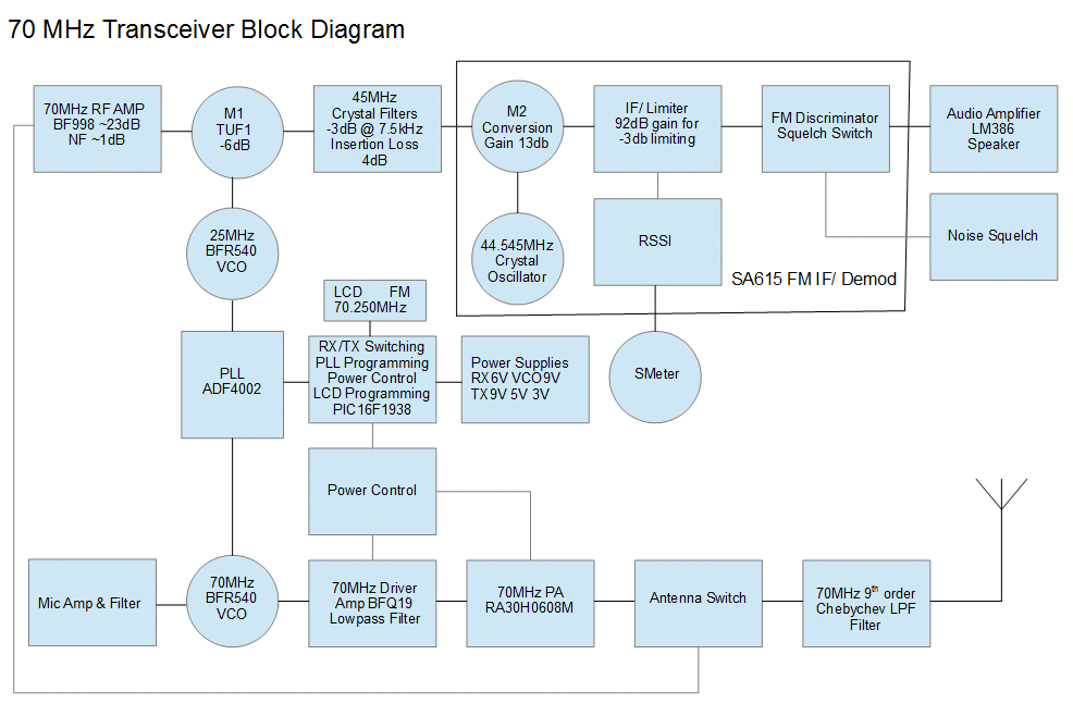
The block diagram above shows I have used the standard double superheterodyne architecture.
The front end pre-amp is designed around a BFR520 low noise UHF transistor and has ~ 23dB of gain. The transistor is biased with around 50mA of collector current to present ~ 50ohms looking into the base. The coupling into the base is via a bandpass filter centered around 70.25MHz. The collector is also presented with 50ohm from a 2nd band pass filter which couples to the RF port of the mixer. The first mixer is a Mini-Circuits TUF1 +7dBm LO drive.
The first IF is at 45MHz and is filtered using a pair of Golledge 45G7B1 crystal filters. The LO is produced from a 25MHz Colpitts VCO followed by a buffer formed with a BF998 dual gate MOSFET which is delivering ~ 20mW.
The output of the 45MHz crystal filters is coupled into the 2nd mixer on the SA615 FM IF Subsystem. The SA615 IF has ~ 110dB of gain including the mixer conversion gain and the ceramic filter losses for the 455kHz 2nd IF/Limiter. The discriminator tank is formed by a 270uH tune-able inductor resonated to 455kHz using a 470pF and an 82pF capacitors in parallel.
The squelch signal is generated by passing the discriminator output though a high pass filter to generate a DC switching signal when no signal is present. The DC squelch signal is passed to the SA615 squelch enable pin to produce muted audio when no signal is present. The audio from the muted audio output of the SA615 is then passed through a low pass filter and then to an LM386 to drive the speaker.
Transmitter Description
The audio from the microphone is passed through a pre-amp and filtered to give a response of 300Hz to 3kHz. The audio level swings ~ 2vpp sitting on 2.5V. This used to modulate the TXVCO and TXCO. The TCXO is a Golledge 14.85MHz TCXO I recycled.
The TXVCO is a Colpitts oscillator followed by a BF998 buffer which delivers ~ 20mW at the transmitter frequency (70 – 70.5MHz). The output of the buffer is passed through a 70.25MHz bandpass filter with an insertion loss of ~4.5 dB.
The output of the filter is then split between the PLL and transmit strip. The transmitter next stage is a BFR520 amplifier to produce ~ 10mW which drives the PA driver using a BFQ19 to produce 50mW which is used to drive a PA Module an RA30H0608M the output of the module will be in the order of 30W. This is then passed through an RF switch, power detector and 9th order Chebychev low-pass filter out to the antenna.
PLL Frequency Control
The PLL IC selected is the Analog Devices ADF4002 which will operate up to 400MHz. The ADF4002 is controlled by a PIC16F1938 via an SPI bus which writes the frequency information to the PLL and writes the frequency to an LCD display and to an external memory. The frequency is changed using a rotary encoder which is read by the PIC16F1939 and used to update the frequency information.
Radio Switching
Receive and transmit switching will be handled by the PIC as well as keeping an eye on the VCO's to make sure they are in lock. It will not enable the transmitter until the TX VCO is in lock to avoid transmitting out of band.

