
PDF Downloads
Transmitter Description
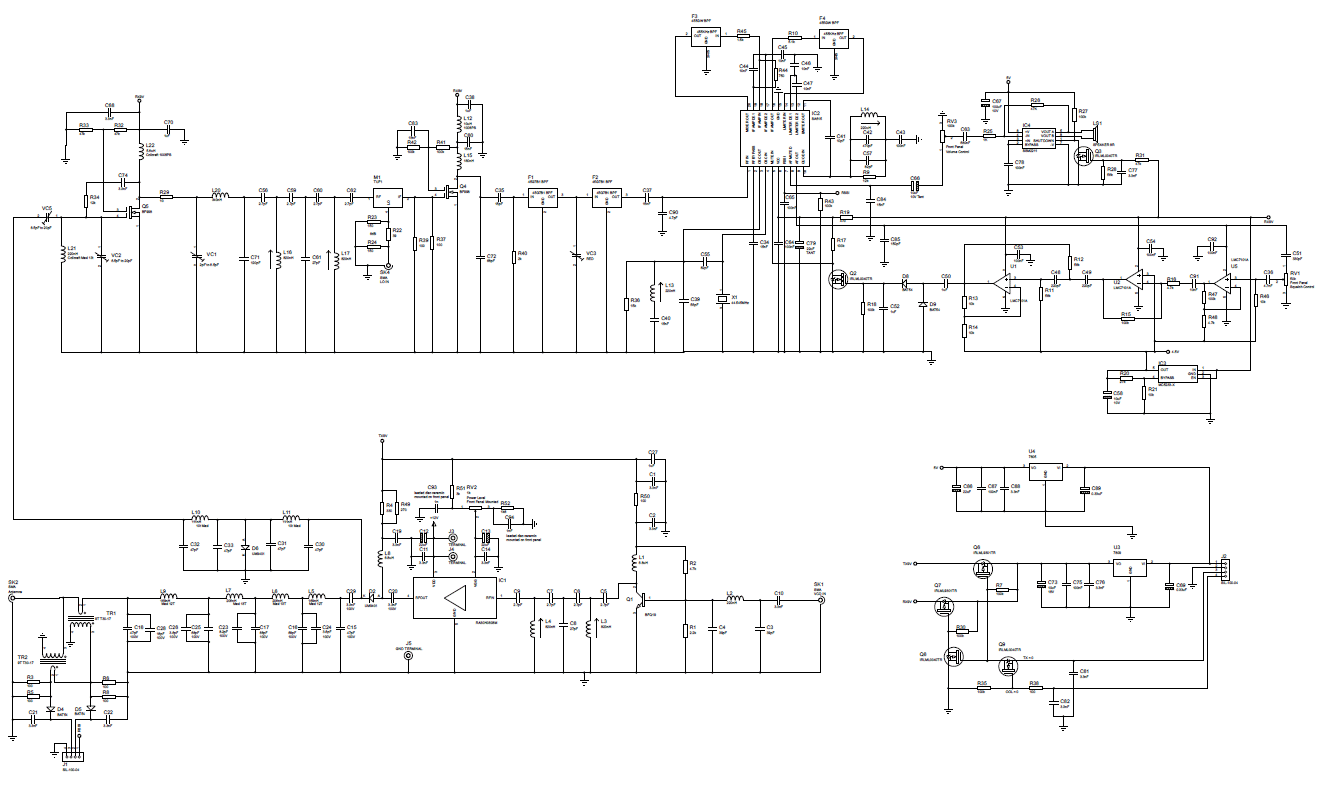
Modulated RF is applied via SK1 which is then passed through a lowpass filter L2 C3,4 to the drive amplifier Q1 a BFQ19. The output of the BFQ19 is passed through a bandpass filter formed by L3/4 and C5,6,7,8,9. The drive amplifier provides ~ 13dB of gain and can deliver ~200mW. The input to the drive amplifier will be set on the synthesizer board to give ~ 50mW out of the drive amplifier to drive the PA module an RA30H0608M which can provide 30W. The PA module will be run at 25W. The power from the PA module will be controlled by front panel mounted RV2. The output from the PA module will then pass through a PIN diode switch D1,2,3,5,7 controlled by 9VTX. Multiple diodes are used in the PIN switch to lower the impedance through the switch to lower the switch power dissipation. The signal then pass through a 9th order Chebychev LPF L5,6,7,9 C15,16,17,18,23,24,25,26,28. The RF then passes through an SWR bridge formed by TR1,TR2 R3,5,6,8 D4,5 BAT54's C21,22 the DC from SWR bridge is connected to the control board where the PIC will monitor and display the SWR on the front panel LCD. The RF is then connected to SK2 and aerial.
Receiver Description
A signal is applied to SK2 from an aerial which passes through the SWR bridge TR1,2 and the Chebychev LPF it then passes through 2 1/4 wave transformers. When the TX9V is present D6,7 are forward biased providing a low impedance to ground and a high impedance on the other side of the transformers preventing transmitter power getting to the receiver. The signal then amplified by the BF998 Q5 low noise pre-amp which has 1dB noise figure and a gain of~ 23dB. The signal then passes through a BPF L16.17 C56,59,60,61,62 which has ~ 4.5dB insertion loss. The signal in then applied to a TUFF1 double balanced mixer which has a conversion loss of ~ 6dB. The local oscillator is provided by the synthesizer board at a level of +7dBm. The output of the mixer is filter by a pair of 45MHz crystal filters with a 7.5kHz bandwidth and an insertion loss of ~ 4dB. So the signal gain at this point will be ~ 7dB tacking into account the losses through the Chebychev LPF and 1/4 wave transformers.
This signal is the applied to the SA615 FM IF subsystem IC. The SA615 has a sensitivity of - 118dBm for 12dB SINAD. So the receiver should be able to hear down to -125dBm for 12dB SINAD. The SA615 has an on board mixer which mixes the 45HMz first IF down to 455kHz. X1 provides the local oscillator signal for this mixer. F3,4 provide 455kHz band pass filtering. L14 tunes the 455kHz quadrature discriminator for maximum audio.
A noise squelch is provided by RV3(front panel mounted) U1,2 Q3,4 U1 provide a gain of 10 to the unfiltered signal from SA615 demodulator. U2 forms a high pass filter with a cutoff of ~ 4kHz the amplified high frequency noise is the rectified and filtered by D8 C57 and used to switch Q3 on Q4 inverts the signal on Q3 drain to provide a signal to mute the audio from the SA615. The switched audio is amplified by IC5 an SSM2211 to drive a 8ohm loud speaker with up to 1.5W of audio. RV4 provides a front panel volume control.
Power Supplies
12V is supplied to the board through J2. The 9V supply is generated using a series regulator U3 a 7809 500mA in DPAK. The TX9V and RX9V are provided by Q6 and Q7 IRLML9301TR MOSFETs. The TX9V signal is prevented from being active unless the OOL signal from the synthesizer board is not present. If OOL = +5V then transmit is enabled by Q9 if OOL = 0V Q9 Prevents the TX9V from being active. U4 a 5V 7805 500mA DPAK provides 5V for IC5 the SSM2211 audio amplifier.
Schematic Update 02/08/16
The circuit has been updated to correct for a couple of problems which showed up while testing the PCB. The 44.545MHz oscillator was re designed to improve start up. This required the inductor L13 to be moved to the junction of C39,55 and the addition of a bias resistor R36. The squelch circuit had Q4 removed which was giving an inversion to the squelch input on the SA615 which was not needed. The 45MHz IF has been given a pre amp Q4 BF998 and the match from the filters to the SA615 input has be changed to an L match.
Schematic Update 29/09/16
PIN diodes were replace with UM9401 from Microsemi. This was due the BAP64-2 going up in smoke in the transmit path. The bias current to the PIN diodes doubled to ~50mA by adding a 270 resister in parallel with R4 330. This was done to minimize losses through the diodes. Padding added for the power control 3k to +5V 1.8k to ground. This was done to spread the range over the full range of the power control. Post mixer amplifier Q4 drain load changed to 45MHz tuned circuit to improve the gain. R40 added to match the input to the 45MHz filter to 2k. L15 removed as it was not required. The squelch amplifier gain changed to 400 by the adition of a LM7101. This was done to improve the squelch range.
24/10/16
Reflection power transformer need screening transformer being swamped by high RF field.
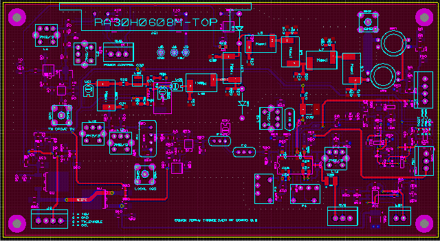
MAIN RF PCB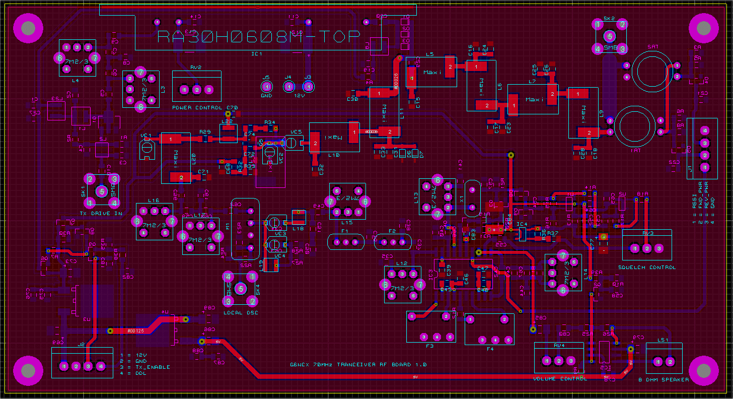
PCB Update 02/08/16
The PCB was updated to reflect the changes in the schematic and to resolve a more serious problem which was the SA615 IF/Limiter was oscillating at 457kHz. It was not possible to fix the problem without changing the PCB layout. The gain of the SA615 IF has been reduced. The 45MHz pre-amp was added to compensate for the additional loss in the SA615 455kHz IF. To improve ground impedance via stitching was added between the top and bottom ground planes.
PCB Update V2.0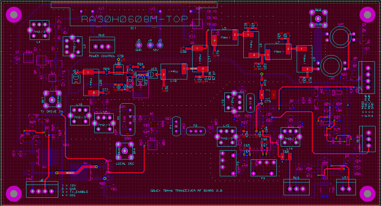
PCB Update 29/09/16
The PCB was updated to reflect the latest changes in the Schematic Update 29/09/16. This is expected to be the final transmitter PCB.